


Thin-film thickness control across industries
Film thickness decides whether a cell converts, a chip yields, or a coating works. We measure that layer on PV, semiconductor, and optics lines — early enough to hold the process.
All Solutions


Thin-film metrology for lab and production
Offline, inline and in-situ film metrology, plus PV reliability testing and inkjet process tools.
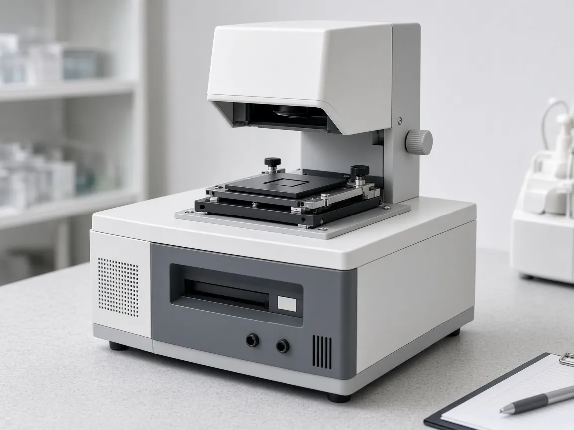
Defect Mapping Instrument
Defect mapping for thin-film surfaces.
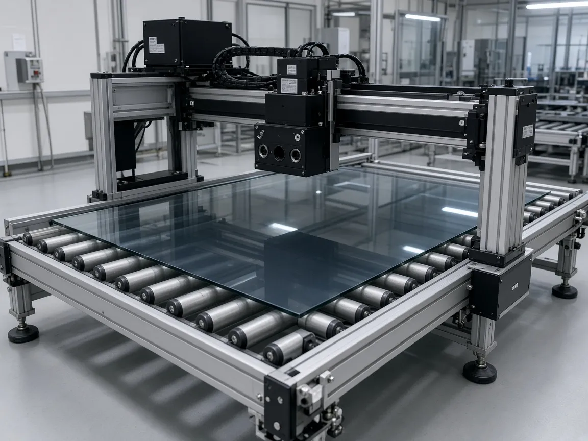
Inline Perovskite Thickness, PL and T&R
Inline perovskite thickness, PL and transmittance/reflectance.
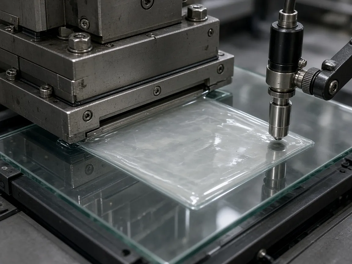
Slot Die Wet Film Metrology Module
Coating-head wet-film thickness & reflectance.
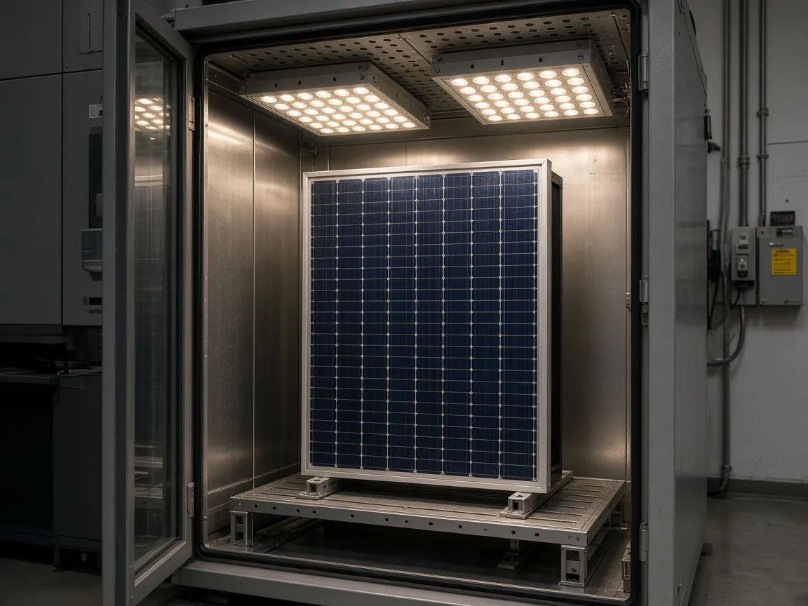
PV Module Light Degradation Tester
Light degradation testing for PV modules.

- Spectroscopic Ellipsometry for Thin Film Metrology Guide2026/9/14
- Inline perovskite metrology demos available in Plano2026/8/18
- 24h technical response channel for installed-base customers2026/7/2
- Inline vs offline metrology: choosing the right stage2026/5/10
- US spare parts and FIFO fulfillment for installed tools2026/4/2
US-Based, End-to-End Support
Our measurement portfolio covers a broad range of thin-film measurement applications. Local stock, 24-hour response, — on the ground in the U.S.

Perovskite and thin-film focus
Full-stack metrology support for PV, semiconductor, and electronics process lines.

Full-stack metrology support for PV, semiconductor, and electronics process lines.
Local coverage for thin-film metrology — marketing, delivery, and support for running tools.

24-hour technical response
Local application engineering, calibration, spare parts, and repair for the installed base.

Troubleshooting & technical support
Seamless technical support services with seamless communication. We also provide on-site technical support on multi locations per business need.

Let's talk about your film process
Talk to Techcess about thin-film metrology, U.S. inventory, and application support.